Microprocessor Design
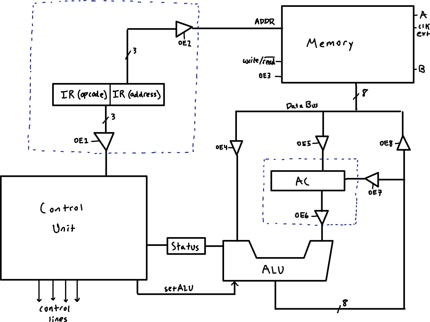 As a part of the microelectronics coursework module at the University of Oxford, I worked with a team of three others to design an 8-bit microprocessor. Our first challenge was to come up with an architecture that could be implemented in the time that we had. We decided to forgo the usual instruction fetch process in favor of a simpler direct instruction loading process. With the three bit opcode, we were therefore able to implement the following instructions:
- Null
- Load
- Store
- Add
- And
- Or
- Not
- BZ (branch if zero)
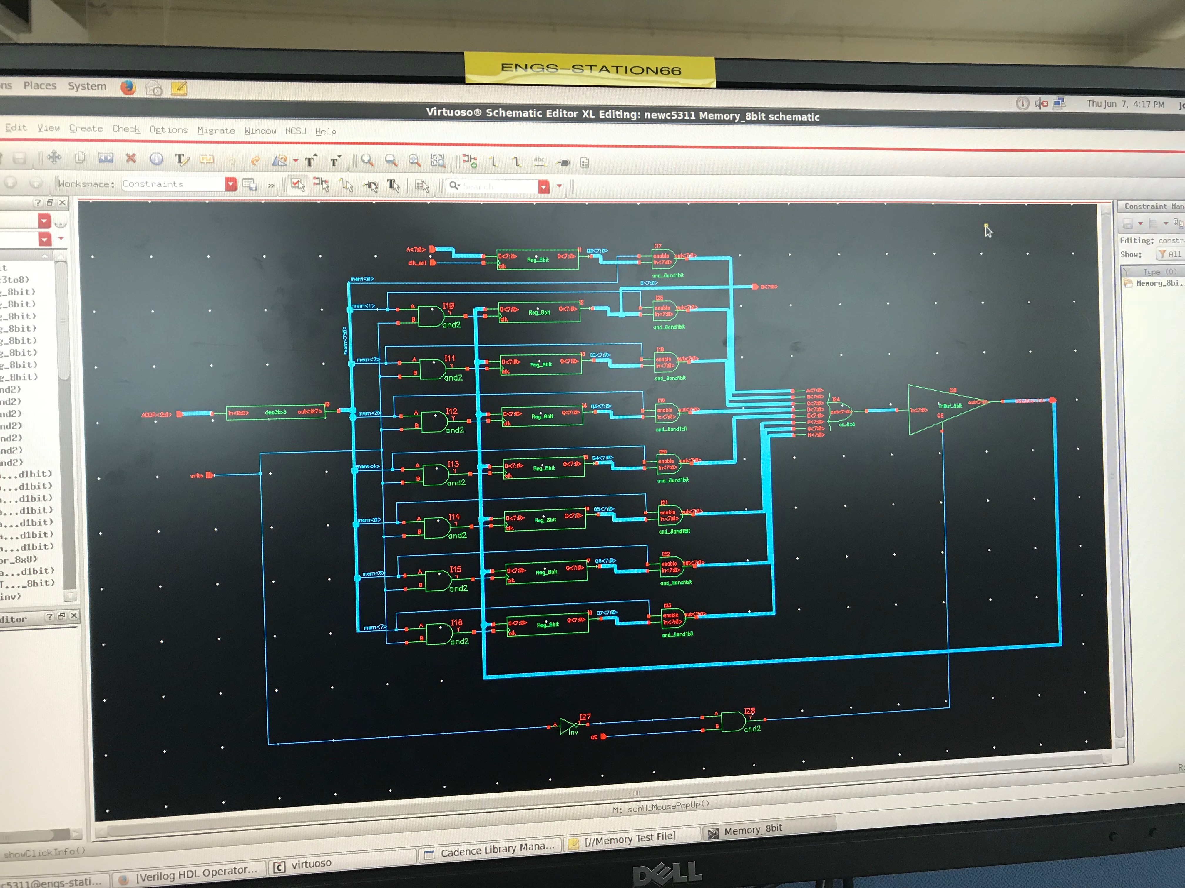 My contribution to the project was the design and schematic entry for the memory module. The memory design included 8 registers and the ability to select a read or write operation. The schematic was created using Cadence Virtuoso. Following the individual design of each module - control unit, arithmetic logic unit, and memory - the microprocessor was assembled in Virtuoso and tested for accuracy.